




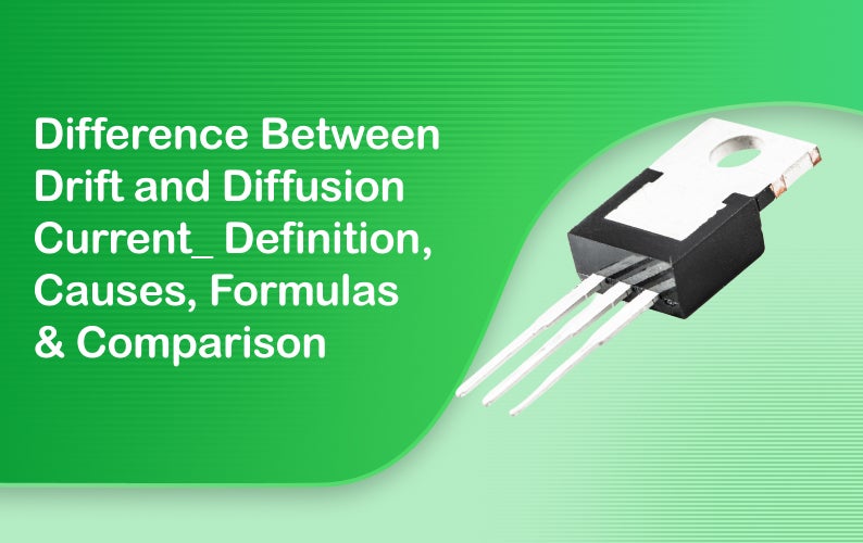
Difference Between Drift and Diffusion Current: Definition, Causes, Formulas & Comparison
Summary
Semiconductor devices rely on two distinct transport mechanisms to move charge. One flows when an electric field pushes carriers along a set path. The other arises when carriers spread from crowded regions toward emptier ones. Together, drift current and diffusion current explain how diodes, transistors, and solar cells actually work. Understanding what is diffusion current and drift current, and how drift and diffusion current in semiconductor devices interact, makes circuit behaviour far easier to predict.
Key Takeaways
• One mechanism needs an external electric field. It pushes carriers in one direction.
• The other needs no external field. It happens on its own, from high to low concentration.
• Understanding what is diffusion current and drift current comes down to what drives the motion, not the carriers themselves.
• Both mechanisms operate together inside a PN junction. They balance each other at equilibrium.
• Formulas for each transport type use different variables. One uses mobility and field. The other uses diffusion constants and gradients.
• Real devices like BJTs, diodes, and solar cells depend on this balance to work correctly.
Introduction
Every semiconductor device depends on charge carriers moving in a controlled way. That includes a simple diode. It includes a solar panel too. That movement does not happen randomly. Two separate forces are usually at work, each pulling carriers in its own way. One force comes from an applied voltage. Think of what pushes electricity through the wiring feeding an electrical socket. The other comes from something quieter. Carriers simply spread out because too many are crowded in one spot. This article walks through what is diffusion current and drift current and the difference between them.
Understanding Charge Carrier Dynamics in Semiconductors
Charge carriers inside a semiconductor rarely move for just one reason. Drift current and diffusion current usually act at the same time. Sometimes they reinforce each other. Sometimes they cancel out. One depends on an external push. The other depends purely on how carriers are spread inside the material. Grasping both is the starting point for understanding how nearly every semiconductor device actually works.
Drift current is the flow of charge carriers driven by an applied electric field. Diffusion current is the motion of carriers driven by a concentration gradient, with no external field required.
These two mechanisms, diffusion and drift current together, govern how current flows inside diodes, bipolar junction transistors, and photovoltaic cells. In a diode, the balance between them at the junction decides whether current flows freely or gets blocked. In a BJT, both mechanisms shape how carriers cross the base region. In a solar cell, light-generated carriers rely partly on one mechanism just to reach the external circuit. Without this interplay, none of these parts would behave the way engineers expect.
What is Drift Current?
Think about this as the more intuitive of the two mechanisms. An external voltage creates an electric field inside the semiconductor. That field pushes charge carriers along a set path. Electrons move against the field direction. Holes move along it. The result is a directional flow of charge that depends on voltage.
Driving Force and Mechanism
An applied voltage across a semiconductor sets up an electric field inside the material. This field applies a force on every free carrier present. Electrons carry negative charge, so they accelerate opposite to the field direction. Holes carry positive charge, so they move the same way as the field. This directional push makes the resulting current controllable and predictable. A higher applied voltage means a stronger field. A stronger field means faster carrier movement, almost in direct proportion.
Key Formula for Drift Current Density
Here is the step-by-step logic behind this field-driven mechanism. It combines the contribution from electrons with the contribution from holes. The total current density is expressed as:
(Where q = electron charge, n/p = carrier concentrations, μn/μp = mobility, E = electric field).
What is Diffusion Current?
Not every current inside a semiconductor needs a push from outside. This one happens when carriers naturally spread from a crowded region into a sparse one, purely because of concentration differences. No external voltage triggers it. In reality, it behaves a lot like a scent slowly filling an empty room. Carriers simply move toward where there is more space, until the concentration evens out. This mechanism plays a key role in how PN junctions build their internal electric field in the first place.
Driving Force and Concentration Gradients
Carriers naturally spread from regions of high concentration to regions of low concentration. No external voltage is needed for this to happen. It is simply a statistical tendency, much like particles in any medium drift toward areas with more empty space. Inside a semiconductor, if electrons or holes pile up unevenly, this spreading kicks in right away. It continues until the imbalance disappears, or until some opposing force, like an internal field, holds it in check.
Key Formula for Diffusion Current Density
This gradient-driven current follows Fick's First Law, adapted for semiconductor carriers. The total current density is expressed as:
Jdiff = qDn ( dn dx ) − qDp dp dx
(Where Dn/Dp = diffusion constants, dn/dx / dp/dx = concentration gradients).
Difference Between Drift and Diffusion Current
At this point, the difference between drift and diffusion current should feel less abstract. One mechanism needs an external field to get moving. The other happens on its own, driven purely by concentration imbalance. Temperature and mobility affect each mechanism in different ways too, and the governing equations rely on entirely separate variables. The table below lays out these contrasts side by side, so the comparison is easy to scan at a glance.
| Parameter | Field-Driven Transport | Concentration-Driven Transport |
|---|---|---|
| Driving Force | Applied electric field | Concentration gradient |
| External Voltage Requirement | Required | Not required |
| Carrier Direction | Follows field direction (holes) or opposes it (electrons) | Moves from high to low concentration |
| Dependence on Temperature/Mobility | Strongly dependent on carrier mobility | Strongly dependent on diffusion constant, which itself depends on temperature |
Behavior of Drift and Diffusion Current in Semiconductor Components
Inside real devices, drift current and diffusion current rarely act alone. They interact constantly. Sometimes they reinforce each other. Sometimes they pull in opposite directions entirely. A PN junction is the clearest example of this. One mechanism builds an internal field there. The other balances against it at equilibrium. Applying an external bias shifts that balance one way or the other. The sections below cover how this plays out inside real components, from simple junctions to working devices like solar cells and transistors.
Dynamics in a PN Junction Depletion Region
At a PN junction, carriers naturally spread across the boundary. This forms what is known as the space charge region. That spreading builds a built-in potential, an internal electric field that opposes further imbalance. At thermal equilibrium, this internal field generates a matching field-driven flow. It balances the concentration-driven flow exactly. Neither mechanism wins out. The junction settles into a stable state, with net current across the boundary equal to zero.
Forward Bias vs. Reverse Bias Equilibrium
Applying forward bias reduces the built-in potential. This weakens the internal field and lets more carriers spread across the junction. So the concentration-driven flow takes over, and current rises sharply. Reverse bias does the opposite. It strengthens the internal field, which suppresses the concentration-driven flow almost entirely. What remains is a small, field-driven leakage current. This shift in balance is exactly what gives diodes their asymmetric switching behaviour.
Real-World Applications
Solar cells depend on this balance to push light-generated carriers toward the external circuit, generating usable power. Bipolar junction transistors rely on carriers crossing the base region, where both mechanisms shape amplification. Diodes use the same balance to allow current in one direction while blocking it in the other. Whether the device is powering a factory circuit or a home electrical socket, this interaction sits quietly behind almost every semiconductor component in use today.
Conclusion
Charge transport inside a semiconductor rarely comes down to a single cause. Grasping diffusion and drift current as a linked pair matters. So does understanding how drift and diffusion current in semiconductor devices actually behave together. Real devices lean on both mechanisms at once. Diodes, transistors, and solar cells all owe their behaviour to this interplay, whether carriers are settling into equilibrium at a junction or shifting under an applied bias. For engineers and students who want to explore the components and panels that these principles ultimately power, from the smallest circuit board to a household electrical socket, the Schneider Electric eShop offers a dependable range worth browsing for related electrical and control gear.
FAQs
Q1. Can the two current components cancel each other out completely?
Yes, this happens at thermal equilibrium inside an unbiased PN junction. The two opposing flows balance exactly. Net current across the junction becomes zero, even though both mechanisms stay active.
Q2. Which mechanism dominates in a heavily doped semiconductor?
Heavily doped regions often show stronger concentration-driven effects near junctions, since the sharp doping difference creates a steep gradient. Away from junctions, field-driven effects tend to take over once an external voltage is applied.
Q3. Does temperature affect both mechanisms equally?
No. Diffusion constants rise with temperature, following the Einstein relation. Mobility, which governs the field-driven mechanism, usually drops as temperature rises, due to more frequent carrier collisions.
Q4. Why does reverse bias produce only a small leakage current?
Reverse bias strengthens the internal junction field. This suppresses the concentration-driven flow almost entirely. What remains is a small, field-driven current from minority carriers, which is why reverse leakage stays low.
Q5. Are diffusion and drift current relevant outside semiconductor physics?
Yes, in principle. The same idea, movement caused by a driving force versus movement caused by concentration imbalance, shows up in other transport processes too, including some models of heat flow and particle movement in gases and liquids.
Comments